- 您现在的位置:买卖IC网 > Sheet目录1997 > ICS650G-40ALFT (IDT, Integrated Device Technology Inc)IC CLOCK ETHERNET SWITCH 16TSSOP
ICS650-40A
ETHERNET SWITCH CLOCK SOURCE
CLOCK SYNTHESIZER
IDT / ICS ETHERNET SWITCH CLOCK SOURCE
3
ICS650-40A
REV E 051310
External Components
A minimum number of external components are required for proper operation. Decoupling capacitors of 0.01
F
should be connected between VDD and GND pairs. The capacitors should be placed between pins VDD and GND,
VDDOA and GND, and VDDOB and GND as close to the device as possible. A 33
series terminating resistor
should be used on each clock output if the trace is longer than 1 inch. A 25 MHz fundamental mode parallel
resonant crystal should be used with CL=18 pF.
On chip capacitors. On Chip capacitors are used for a 18 pF load crystal. Small, 2-3 pF trimming capacitors are
used from pins X1 to ground and X2 to ground to optimize the initial accuracy.
Absolute Maximum Ratings
Stresses above the ratings listed below can cause permanent damage to the ICS650-40A. These ratings, which are
standard values for IDT commercially rated parts, are stress ratings only. Functional operation of the device at these
or any other conditions above those indicated in the operational sections of the specifications is not implied.
Exposure to absolute maximum rating conditions for extended periods can affect product reliability. Electrical
parameters are guaranteed only over the recommended operating temperature range.
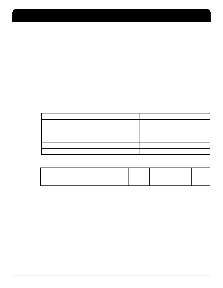
Recommended Operation Conditions
Item
Rating
Supply Voltage, VDD
7 V
All Inputs and Outputs
-0.5 V to VDD+0.5 V
Ambient Operating Temperature
0 to +70
° C
Storage Temperature
-65 to +150
° C
Junction Temperature
125
° C
Soldering Temperature
260
° C
Parameter
Min.
Typ.
Max.
Units
Ambient Operating Temperature
0
+70
° C
Power Supply Voltage (measured in respect to GND)
+3.15
+3.45
V
发布紧急采购,3分钟左右您将得到回复。
相关PDF资料
ICS650GI-44LF
IC CLK SYNTHESIZER 16-TSSOP
ICS650GI-47LF
IC CLK SYNTHESIZER 16-TSSOP
ICS650R-12LF
IC MPEG CLK SYNTHESIZER 20-SSOP
ICS650R-14LFT
IC NETWORKING SYSTEM CLK 20-SSOP
ICS650R-21ILF
IC CLK SOURCE SYSTEM PER 20-SSOP
ICS650R-22LF
IC CLK SOURCE PRV/STB 20-SSOP
ICS650R-27ILF
IC CLK SOURCE NETWORK 20-SSOP
ICS663MILFT
IC PLL BUILDING BLOCK 8-SOIC
相关代理商/技术参数
ICS650G-40AT
功能描述:IC CLOCK ETHERNET SWITCH 16TSSOP RoHS:否 类别:集成电路 (IC) >> 时钟/计时 - 时钟发生器,PLL,频率合成器 系列:- 产品变化通告:Product Discontinuation 04/May/2011 标准包装:96 系列:- 类型:时钟倍频器,零延迟缓冲器 PLL:带旁路 输入:LVTTL 输出:LVTTL 电路数:1 比率 - 输入:输出:1:8 差分 - 输入:输出:无/无 频率 - 最大:133.3MHz 除法器/乘法器:是/无 电源电压:3 V ~ 3.6 V 工作温度:0°C ~ 70°C 安装类型:表面贴装 封装/外壳:16-TSSOP(0.173",4.40mm 宽) 供应商设备封装:16-TSSOP 包装:管件 其它名称:23S08-5HPGG
ICS650G-40LF
功能描述:IC CLOCK ETHERNET SWITCH 16TSSOP RoHS:是 类别:集成电路 (IC) >> 时钟/计时 - 时钟发生器,PLL,频率合成器 系列:- 产品变化通告:Product Discontinuation 04/May/2011 标准包装:96 系列:- 类型:时钟倍频器,零延迟缓冲器 PLL:带旁路 输入:LVTTL 输出:LVTTL 电路数:1 比率 - 输入:输出:1:8 差分 - 输入:输出:无/无 频率 - 最大:133.3MHz 除法器/乘法器:是/无 电源电压:3 V ~ 3.6 V 工作温度:0°C ~ 70°C 安装类型:表面贴装 封装/外壳:16-TSSOP(0.173",4.40mm 宽) 供应商设备封装:16-TSSOP 包装:管件 其它名称:23S08-5HPGG
ICS650G-40LFT
功能描述:IC CLOCK ETHERNET SWITCH 16TSSOP RoHS:是 类别:集成电路 (IC) >> 时钟/计时 - 时钟发生器,PLL,频率合成器 系列:- 产品变化通告:Product Discontinuation 04/May/2011 标准包装:96 系列:- 类型:时钟倍频器,零延迟缓冲器 PLL:带旁路 输入:LVTTL 输出:LVTTL 电路数:1 比率 - 输入:输出:1:8 差分 - 输入:输出:无/无 频率 - 最大:133.3MHz 除法器/乘法器:是/无 电源电压:3 V ~ 3.6 V 工作温度:0°C ~ 70°C 安装类型:表面贴装 封装/外壳:16-TSSOP(0.173",4.40mm 宽) 供应商设备封装:16-TSSOP 包装:管件 其它名称:23S08-5HPGG
ICS650G-40T
功能描述:IC CLOCK ETHERNET SWITCH 16TSSOP RoHS:否 类别:集成电路 (IC) >> 时钟/计时 - 时钟发生器,PLL,频率合成器 系列:- 产品变化通告:Product Discontinuation 04/May/2011 标准包装:96 系列:- 类型:时钟倍频器,零延迟缓冲器 PLL:带旁路 输入:LVTTL 输出:LVTTL 电路数:1 比率 - 输入:输出:1:8 差分 - 输入:输出:无/无 频率 - 最大:133.3MHz 除法器/乘法器:是/无 电源电压:3 V ~ 3.6 V 工作温度:0°C ~ 70°C 安装类型:表面贴装 封装/外壳:16-TSSOP(0.173",4.40mm 宽) 供应商设备封装:16-TSSOP 包装:管件 其它名称:23S08-5HPGG
ICS650GI-36
制造商:ICS 制造商全称:ICS 功能描述:Networking & PCI Clock Source
ICS650GI-36LF
功能描述:IC CLOCK NETWORK/PCI 16-TSSOP RoHS:是 类别:集成电路 (IC) >> 时钟/计时 - 时钟发生器,PLL,频率合成器 系列:- 标准包装:1,000 系列:- 类型:时钟/频率合成器,扇出分配 PLL:- 输入:- 输出:- 电路数:- 比率 - 输入:输出:- 差分 - 输入:输出:- 频率 - 最大:- 除法器/乘法器:- 电源电压:- 工作温度:- 安装类型:表面贴装 封装/外壳:56-VFQFN 裸露焊盘 供应商设备封装:56-VFQFP-EP(8x8) 包装:带卷 (TR) 其它名称:844S012AKI-01LFT
ICS650GI-36LFT
功能描述:IC CLOCK NETWORK/PCI 16-TSSOP RoHS:是 类别:集成电路 (IC) >> 时钟/计时 - 时钟发生器,PLL,频率合成器 系列:- 标准包装:2,000 系列:- 类型:PLL 时钟发生器 PLL:带旁路 输入:LVCMOS,LVPECL 输出:LVCMOS 电路数:1 比率 - 输入:输出:2:11 差分 - 输入:输出:是/无 频率 - 最大:240MHz 除法器/乘法器:是/无 电源电压:3.135 V ~ 3.465 V 工作温度:0°C ~ 70°C 安装类型:表面贴装 封装/外壳:32-LQFP 供应商设备封装:32-TQFP(7x7) 包装:带卷 (TR)
ICS650GI-36T
制造商:ICS 制造商全称:ICS 功能描述:Networking & PCI Clock Source